|
Keynote & Invited Speakers(2021)
|
|
|
|
|
|
|
|
|
|
|
|
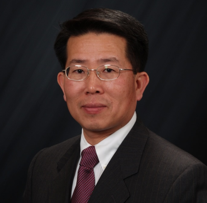
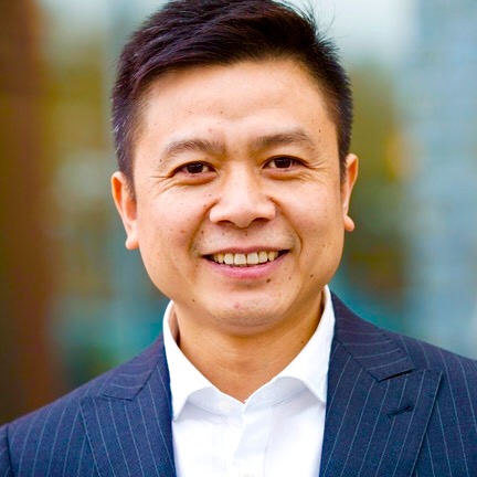
Driving and Delivering High Performance Compute and Graphics Solutions
Mr. Allen Lee, Corporate Vice President, GM of China R&D Center, AMD
|
|
|
|
|
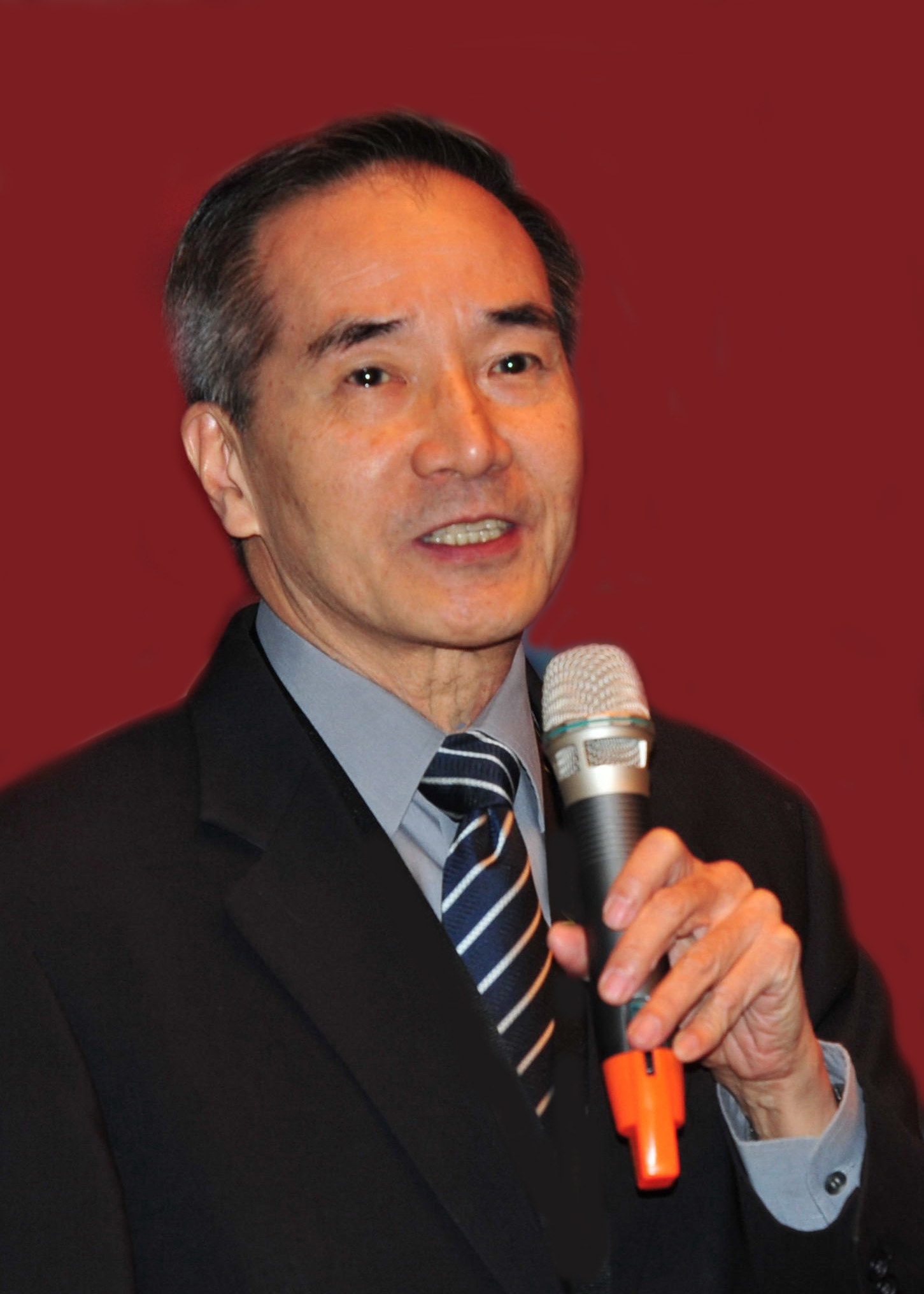
Nanolithography Milestones and Future
Dr. Burn J. Lin, CEO, Linnovation, Inc
|
|
|
|
|
|
|
|
|
|
|
|
|
|
|
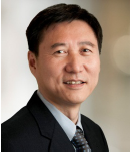
Ferroelectric Field Effect Transistor: A Novel Computational Memory
Dr. Suman Datta, Professor, University of Notre Dame
|
|
|
|
|
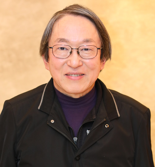
Enabling Specialty Applications in the IoT Era
Dr. Zheng Yuan, Vice President and General Manager, Specialty Products and Technology, Applied Materials, Inc
|
|
|
|
|
|
|
|
|
|
|
|
|
|
Partial List of Confirmed Distinguished CSTIC 2021 Invited Speakers
|
|
|
|
|
|
|
|
|
|
|
|
|
High Yield and Superior Quality/Reliability of IGBT and Power Devices at AI Era
Minhwa Chi, SVP, SiEn (Qindao) Integrated circuits, China
|
|
|
|
|
Frontiers in Low-frequency Noise Research in Advanced Semiconductor Devices
Eddy Simoen, IMEC and University of Gent, Belgium
|
|
|
|
|
|
|
|
|
|
|
|
|
|
|
Innovative Future Etch Technology by Atomic-order Control
Yoshihide Kihara, Director, Tokyo Electron Limited, Japan
|
|
|
|
|
The Latest Development and Results in Advanced Technoogy Nodes Patterning
Rich Wise, Lam Research, US
|
|
|
|
|
|
|
|
|
|
|
|
|
|
|
Advanced Packaging Architectures for Advanced Heterogeneous Integration (HI)
Ravi Mahajan, Fellow, Intel
|
|
|
|
|
A New Generation Cost-efficient Laser Mask Writer for Mature Semiconductor Nodes
Peter Henriksson, System Architect, Mycronic AB
|
|
|
|
|
|
|
|
|
|
|
|
|
|
|
2-D Logic Device Scaling to Forksheet, and Technical Challenges to Nanosheet / Forksheet Configurations
David Xiao, Program Manager of Core CMOS scaling, IMEC, Belgium
|
|
|
|
|
Advanced Dry Removal Technology for Patterning
Hua Chuang, VP, Mattson, US
|
|
|
|
|
|
|
|
|
|
|
|
|
|
|
The Latest Development and Results on CCP Etch Applications
Xingcai Su, GM, AMEC, China
|
|
|
|
|
Advanced Materials and Process Technology for Patterning
Ajay Bhatnagar, Sr. Director, Applied Materials, US
|
|
|
|
|
|
|
|
|
|
|
|
|
|
|
Perspective on Plasma Etching in Advanced Packaging
Dr. Yuanwei Lin, Process Engineer, NAURA, Beijing, China
|
|
|
|
|
Patterning Challenges andPerspetive Solutions for Advanced Technology Nodes
Da Yang, Director, Tokyo Electron Limited, US
|
|
|
|
|
|
|
|
|
|
|
|
|
|
|
Practical Solutions to the Challenges of Quantitative Radical Species Sensoring in Process Plasmas
Jianping Zhao, SMTS, Tokyo Electron America, US
|
|
|
|
|
New Frontiers of Device Fabrication with Atomic Precisio
Peter Ventzek, Senior Manager, Tokyo Electron Limited, US
|
|
|
|
|
|
|
|
|
|
|
|
|
|
|
Fin Self-Aligned Quadruple Patterning (SAQP) Process Development with Domestic Made Tools
Yushu Yang, Shanghai IC R&D Center, China
|
|
|
|
|
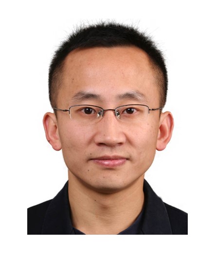
Hardware/Software Co-Design of Deep Learning Accelerators
Yiyu Shi, Associate Professor, University of Notre Dame, US
|
|
|
|
|
|
|
|
|
|
|
|
|
|
|
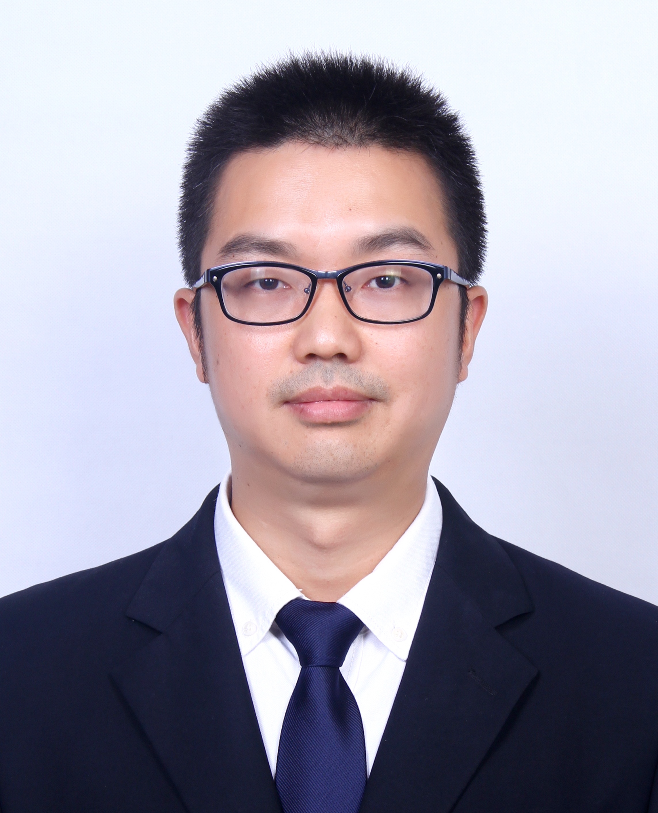
Multi-GPU Acceleration for Global Placement
Yibo Lin, Assistant Professor, Peking University, China
|
|
|
|
|
Advancing to the Next Node and Competing Globally Using Virtual Fabrication
Joseph Ervin, Director, Lam Research
|
|
|
|
|
|
|
|
|
|
|
|
|
|
|
Monolithic Integration of Thin Film Photodiode with CMOS Technology for Infrared Imaging Applications
Yunlong Li, Senior R&D Engineer, IMEC, Belgium
|
|
|
|
|
Keys to Extending Cu Interconnect to 3 nm and Shift to Alternative Conductor
Takeshi Nogami, IBM Research
|
|
|
|
|
|
|
|
|
|
|
|
|
|
|
Theoretical and Experimental Approach to Design CVD/ALD Processes
Yukihiro Shimogaki, Tokyo University, Japan
|
|
|
|
|
Area Selective Deposition: fundamentals and applications
Silvia Armini, IMEC, Belgium
|
|
|
|
|
|
|
|
|
|
|
|
|
|
|
Application Investigation of Co-Ti Alloy as Single Liner/Barrier in Advanced Co Interconnects
Luo Jun, Professor, IMECAS, China
|
|
|
|
|
Advanced Memory and Logic Patterning Trends and Applied Material’s solutions to meet the Technical Challenges
Dimitri Kioussis, Applied Materials
|
|
|
|
|
|
|
|
|
|
|
|
|
|
|
Galvanic Corrosion Caused by Device Structure in Chemical Cechanical Planarization
Lei Wang, Manager, Hikstor Hangzhou, China
|
|
|
|
|
Electronic Design Automation for Emerging Technologies
Giovanni De Micheli, Professor and Director, EPFL Lausanne, Switzerland
|
|
|
|
|
|
|
|
|
|
|
|
|
|
|
Proactive Supply Noise Mitigation and Design Methodology for
Robust VLSI Power Distribution
Masanori Hashimoto, Professor, Osaka University, Japan
|
|
|
|
|
Valid Test Pattern Identification for VLSI Adaptive Test
Tianming Ni, Associate Professor, Anhui Polytechnic University, China
|
|
|
|
|
|
|
|
|
|
|
|
|
|
|
Advancements on Parasitic Extraction Research and Related Challenges
Wenjian Yu, Associate Professor, Tsinghua University, China
|
|
|
|
|
Ensuring System-Level Resilience for Embedded Systems
Ulf Schlichtmann, Professor, Technical university of Munich, Germany
|
|
|
|
|
|
|
|
|
|
|
|
|
|
|
The Investigation of SiC CMP with High Efficiency
Weili Liu, Professor, Shanghai Institute of Microsystem and Information, China
|
|
|
|
|
Challenges in Chemical Mechanical Polishing and Post CMP Cleaning of GaAs and InP
Baoguo Zhang, Professor, Hebei University of Technology, China
|
|
|
|
|
|
|
|
|
|
|
|
|
|
|
TSV and Hybrid Bonding Solutions for 3D Heterogeneous Integration Packaging Applying in next AI / HPC Era
Albert Lan, Global Sr. Packaging Technical Director, Applied Materials
|
|
|
|
|
The Novel Etching Process for Dense Array Magnetic Tunneling Junctions Manufacturing
Taiyen Peng, Senior Director, Leuven Instruments, China
|
|
|
|
|
|
|
|
|
|
|
|
|
|
|
FEOL Reliability in Gate-All-Around Nanosheet Devices
Miaomiao Wang, Research Staff Member, IBM, US
|
|
|
|
|
Negative-tone imaging (NTI) for advanced lithography with EUV exposure to improve 'Chemical Stochastic'
TORU FUJIMORI, Research Manager, FUJIFILM Corporation
|
|
|
|
|
|
|
|
|
|
|
|
|
|
|
Maskless Optical Nanolithography for Efficient Cross-scale Patterning
Xuanming Duan, Professor, Jinan University, China
|
|
|
|
|
Interconnect-centric Benchmarking of In-memory Acceleration for DNNs
Yu(Kevin) Cao, Professor, Arizona State University(ASU), US
|
|
|
|
|
|
|
|
|
|
|
|
|
|
|
Modeling of Ferroelectric FET
Kai Ni, Assistant Professor, Rochester Institute of Technology, US
|
|
|
|
|
CMOS Device Design With Ferroelectric Materials
Changhwan Shin, Professor, Sungkyunkwan University, Korea
|
|
|
|
|
|
|
|
|
|
|
|
|
|
|
Source/Drain Contact Technology for Next-Generation Field-Effect Transistors
Hyun-Yong Yu, Professor, Korea University, Korea
|
|
|
|
|
High Performance Electronics Based on Ultrathin Novel Channel Materials
Yanqing Wu, Professor, Peking University, China
|
|
|
|
|
|
|
|
|
|
|
|
|
|
|
Trends and Challenges in Multisensory Integration
Ming He, Assistant Professor, Peking University, China
|
|
|
|
|
Full Chip Curvilinear ILT with both Multi-Beam and VSB Mask Writers That Doubles Wafer Process Windows
Leo Pang, Chief Product Officer, D2S, US
|
|
|
|
|
|
|
|
|
|
|
|
|
|
|
Multiscale Contact Behavior in CMP and its Correlation with Polishing Pad Properties
Ping Zhou, Professor, Dalian University of Technology, China
|
|
|
|
|
Explore the pathway on CMP pad with CMC Materials
Rui Ma, CMC
|
|
|
|
|
|
|
|
|
|
|
|
|
|
|
Computation-In-Memory with Memristors for Neuromorphic Computing
Jianshi Tang, Assistant Proferssor, Tsinghua University, China
|
|
|
|
|
Copper corrosion issue analysis and study on advanced cmp process
Lei Zhang, Principal Engineer, Shanghai Huali Integrated Circuit Corporation
|
|
|
|
|
|
|
|
|
|
|
|
|
|
|
Artificial heterostructures enabled by stacking single-crystalline freestanding membranes
Jeehwan Kim, Massachusetts Institute of Technology(MIT), US
|
|
|
|
|
Surface Redox Buffering Effects on FET Based DNA Sensors with a Gold Sensing Gate
Zhen Zhang, Professor, Uppsala University
|
|
|
|
|
|
|
|
|
|
|
|
|
|
|
Far-field optical detection of 10nm Si nanoparticle
Stas Polonsky, Samsung, Russia
|
|
|
|
|
Van der Waals heterostructures for optoelectronic and electronic devices
Kaiyou Wang, Director, State Key Laboratory for Superlattices & Microstructure
|
|
|
|
|
|
|
|
|
|
|
|
|
|
|
Polarization-Sensitive Photodetectors based on 2D Layered Semiconductors
Zhongming Wei, Professor, Institute of Semiconductors, CAS
|
|
|
|
|
Loss Mechanisms of Multi-frequency Whispering Gallery Mode RF-MEMS Resonators
Jinling Yang, Professor, Institute of Semiconductors, CAS
|
|
|
|
|
|
|
|
|
|
|
|
|
|
|
Customizing CMP Pads
Hongqi Xiang, General Manager, Inventech Materials Co., Ltd
|
|
|
|
|
Nanoimprint Performance Improvements for High Volume Semiconductor Manufacturing
Keita Sakai, General Manager, Canon Inc.
|
|
|
|
|
|
|
|
|
|
|
|
|
|
|
Reference Metrology Using 3D-PSD of Post-Etch LWR
Masami Ikota, Application Engineer, Hitachi High-Tech Corp.
|
|
|
|
|
Extending the capability of lithography with mechanical processes
Huigao Duan, System Architect, Hunan University
|
|
|
|
|
|
|
|
|
|
|
|
|
|
|
Update of >300W High Power LPP-EUV Source Challenge III for Semiconductor HVM
Hakaru Mizoguchi, Senior Fellow, Gigaphoton.
|
|
|
|
|
Integrated Optical Metrology Solutions for Advanced IC Fabrication
Jonee Li, Optical BG General Manager, Shanghai Precision Measurement Semiconductor Technology
|
|
|
|
|
|
|
|
|
|
|
|
|
|
|
The Impacts to Lithography Process Windows by Different Pattern Split Methods
Jinhua Min, Senior Engineer, Shanghai IC R&D Center.
|
|
|
|
|
A General PWC GUI automation testing framework--PWC Robot ATF
Annie An, Engineer, ASML
|
|
|
|
|
|
|
|
|
|
|
|
|
|
|
Contour based process characterization, control and hotspot prediction for semiconductor manufacturing
AO CHEN, Technical Marketing Manager, Mentor, a Siemens Business
|
|
|
|
|
ML enhanced full-flow design guided wafer defect analysis and reduction
Qian Xie, Product Engineer, a Siemens Business
|
|
|
|
|
|
|
|
|
|
|
|
|
|
|
193i lithography's path to the future
Stephen Renwick, Director of Imaging Physics, Nikon Research Corp of America
|
|
|
|
|
An innovative graphical platform for real time accurate AEI overlay prediction and rework control
Yaobin FENG, senior director, YMTC
|
|
|
|
|
|
|
|
|
|
|
|
|
|
|
Simulation investigation of resolution enhancement techniques (RETs) for EUV single patterning of logic Via layers in 5nm nodl
Boer Zhu, Technical Engineer, ASML
|
|
|
|
|
Progress and outlook towards High-NA EUV materials
Jara Garcia Santaclara, Architect, ASML
|
|
|
|
|
|
|
|
|
|
|
|
|
|
|
Feed-forward correction of on-product overlay using standalone alignment technology
Masahiko OKUMURA, Assistant Department Manager, Nikon Corporation
|
|
|
|
|
Overlay metrology based on Mueller matrix scatterometry
Hao Jiang, Professor, Huazhong University of Science and Technology
|
|
|
|
|
|
|
|
|
|
|
|
|
|
In-Memory Computing towards the POS/w era ---an algorithm–architecture co-design approach
Li Jiang, Shanghai Jiaotong University
|
|
|
|
|
A Co-Design Framework of Neural Networks and Quantum Circuits Towards Quantum Advantage
Weiwen Jiang, Post-Doctoral Research Associate, University of Notre Dame, US
|
|
|
|
|
|
|
|
|
|
|
|
|
Opportunities and challenges of wet process tools for wafer level package manufacturing driven by 3D technology
David Wang, ACM Research (Shanghai), Inc.
|
|
|
|
|
Improving Design Resilience Against Process and Voltage Variation
Wei-Kai Shih, R&D Manager, Synopsys
|
|
|
|
|
|
|
|
|
|
|
|
|
On Device AI for AR Systems
Meng Li, Facebook Inc., USA
|
|
|
|
|
Chip Level ESD/Latch-up Design Verification Automation
Frank Feng, Director, Synopsys
|
|
|
|
|
|
|
|
|
|
|
|
|
Full Chip Reliability Verification by Netlist Driven Layout Methodology
Jonathan White, R&D Director, Synopsys, US
|
|
|
|
|
Mass Metrology Solution for 3D Process-Monitoring
Jiangtao Hu, Director, Lam Research, US
|
|
|
|
|
|
|
|
|
|
|
|
|
Mid-Infrared Critical Dimension Ellipsometry and Advanced Machine Learning to Address Complex Semiconductor Manufacturing Metrology Challenges
Franklin Wong, Senior Applications Manager, Onto Innovation, US
|
|
|
|
|
The Development of 3D IPDs on Glass Wafer
Daquan Yu, Xiamen Sky Semiconductor Co., Ltd.
|
|