|
Keynote & Invited Speakers(2022)
|
|
|
|
|
|
|
|
|
|
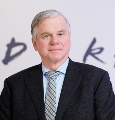
Driving Moore's Law into the Next Decade
Dr. Martin van den Brink, President and Chief Technology Officer, ASML
|
|
|
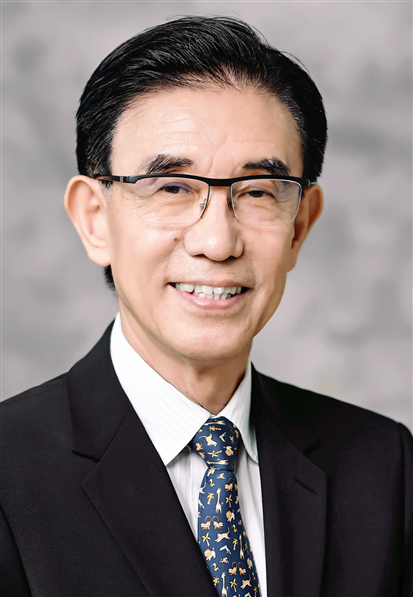
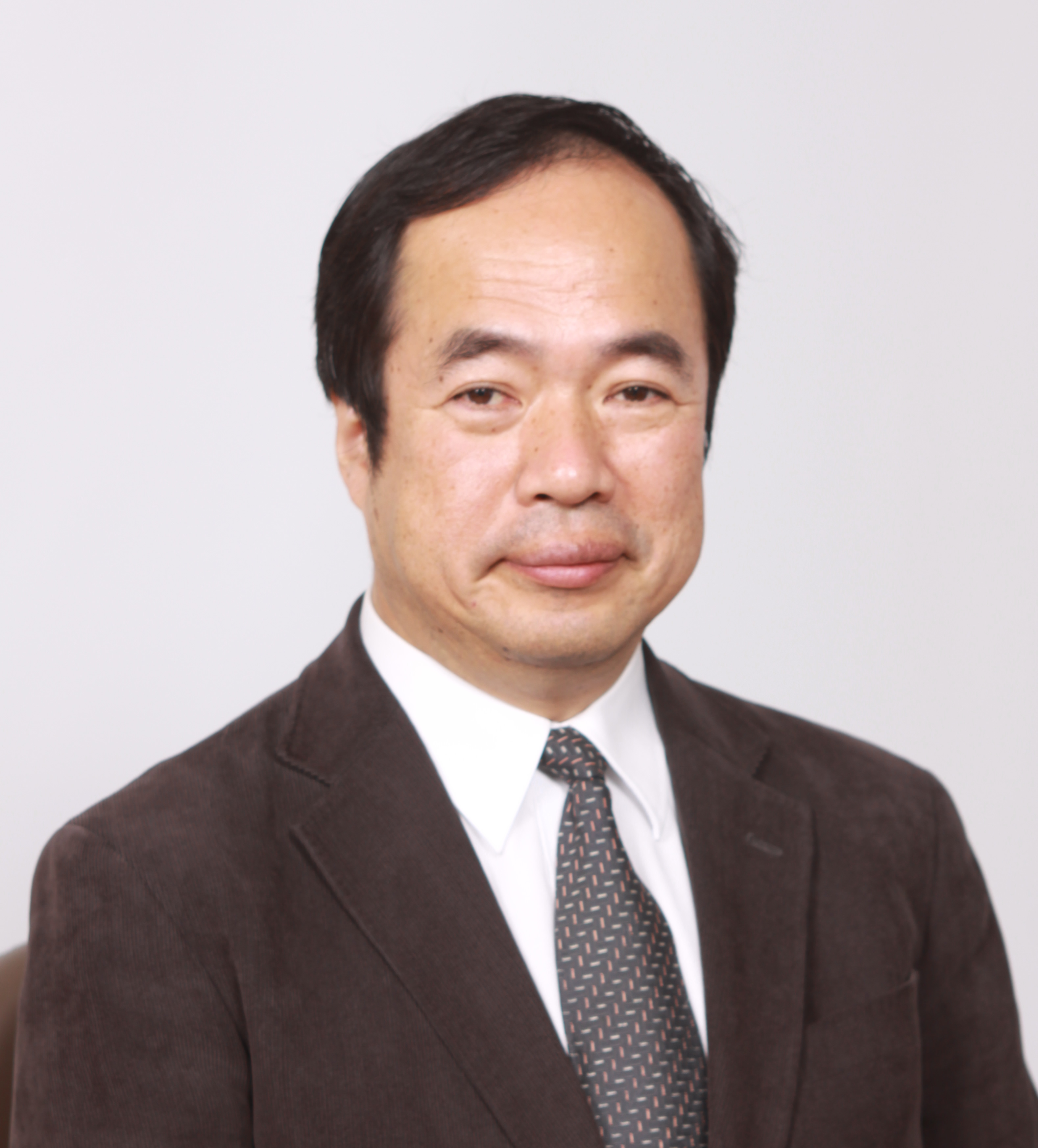
Micro-Fabrication Equipment, the Foundation of Digital Revolution and Beyond
Dr. Gerald Yin, Chairman and CEO, AMEC
|
|
|
|
|
|
|
|
|
|
|
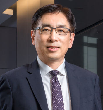
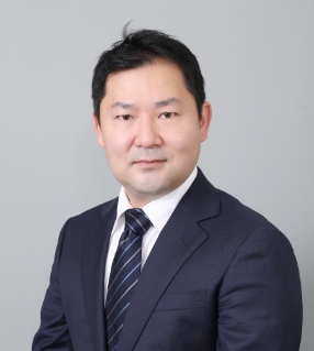
Advanced 3D Chiplet Packaging Technology and Manufacturing
Dr. Marvin Liao, Vice President, APTS, TSMC
|
|
|
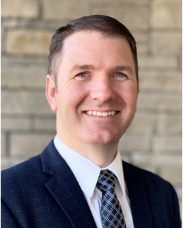
An Innovative 3D HITOC 4F2 DRAM Architecture
Dr. Feng Hong, CEO, ICLeague Technology
|
|
|
|
|
|
|
|
|
|
Partial List of Confirmed Distinguished CSTIC 2022 Invited Speakers
|
|
|
|
|
|
|
|
|
|
Going where silicon cannot reach: Print-in-place and recyclable electronics from nanomaterials
Aaron Franklin, Duke University
|
|
|
Solving Optimization Problems with Nanoelectronic Neuromorphic Circuits
Dmitri Strukov, University of California, Santa Barbara
|
|
|
|
|
|
|
|
|
|
|
Nonvolatile-memory Based Compute-in-memory Technology for Energy Efficient DNN Accelerator
Wonbo Shim, Seoul National University of Science and Technology
|
|
|
Study about self-heating effects in gate-all-around nanowire transistors
Sangwan Kim, Sogang University
|
|
|
|
|
|
|
|
|
|
|
Novel Thermal Material Properties for Post-CMOS Neuromorphic Computing
Suhas Kumar, Sandia National Lab
|
|
|
Low Frequency Noise of Advanced Memory and Logic Devices
Eddy Simoen, Imec, Belgium
|
|
|
|
|
|
|
|
|
|
|
Enabling 3D Monolithic Integration using Oxide-Semiconductor-based Transistors
Xiao Gong, National University of Singapore
|
|
|
The Road to Compatible with and Beyond Silicon Circuits for 2D Materials
Peng Zhou, Fudan University
|
|
|
|
|
|
|
|
|
|
|
Process Window Optimization of DRAM by Virtual Fabrication
Joseph Ervin, Coventor, a Lam Research company
|
|
|
System-technology co-optimization for 3D monolithic memory-centric computing
Bin Gao, Tsinghua University
|
|
|
|
|
|
|
|
|
|
|
Optimization of endurance and operation voltage in ferroelectric field effect transistor memory devices
Kechao Tang, Peking University
|
|
|
Recent Aadvances in Extreme Ultravoliet Photoresists
Guoqiang Yang, Institute of Chemistry, Chinese Academy of Sciences
|
|
|
|
|
|
|
|
|
|
|
Update of >300W High Power LPP-EUV Source Challenge IV for Semiconductor HVM
Hakaru Mizoguchi, Gigaphoton
|
|
|
Patterning capability of surface plasmon imaging
Lihong Liu, Institute of Microelectronics, Chinese Academy of Sciences
|
|
|
|
|
|
|
|
|
|
|
|
EPE and CD performance enhancement by "GT66A", the next-generation immersion ArF lightsource
Takamitsu Komaki, Gigaphoton
|
|
|
Thickness Dependence of Properties of EUV Underlayer Thin Films
Jae-Hwan Sim, DuPont Electronics and Industrial
|
|
|
|
|
|
|
|
|
|
|
Considerations in seting up industry standards for photolithography process, historical perspectives, methologies, and outlook
Qiang Wu, Fudan University
|
|
|
Process window, stochastic defectivity, and process optimization in EUV lithography for advanced logic technologies nodes
Yanli Li, Fudan University
|
|
|
|
|
|
|
|
|
|
|
Nanoimprint Lithography Methods for Achieving sub-3nm Overlay
Keita Sakai, Canon Inc.
|
|
|
Gan-based fast mask near-field calculation
Yijiang Shen, Guangdong University of Technology
|
|
|
|
|
|
|
|
|
|
|
Critical dimension metrology: from OCD to XCD
Xiuguo Chen, Huazhong University of Science and Technology
|
|
|
A new generation cost-efficient laser mask writer, addressable up to the 90nm node
Youngjin Park, Mycronic Co., Ltd.
|
|
|
|
|
|
|
|
|
|
|
Model-driven Deep Learning for Computational Lithography
Xu Ma, Beijing Institute of Technology
|
|
|
Lithography simulation and its applications
Sikun Li, Shanghai Institute of Optics and Fine Mechanics
|
|
|
|
|
|
|
|
|
|
|
Co-Optimization of Photoresist Development and Photolithography Process
Liwan Yue, Ningbo Nata Opto-electronic Materials Co. Ltd
|
|
|
Role of underlayers in novel patterning for EUV lithography
Douglas Guerrero, Brewer Science, Inc.
|
|
|
|
|
|
|
|
|
|
|
Inverse lithography technology: 30 years from concept to practical, full-chip reality
Leo Pang, D2S, Inc.
|
|
|
Advanced Lithography Material Status toward 5nm Node and beyond
Koichi FUJIWARA, JSR Shanghai Co., Ltd.
|
|
|
|
|
|
|
|
|
|
|
3D NAND Technology Cost Scaling Challenge and System Solutions
Richard Yang, Fortune Precision Equipment, China
|
|
|
The fast changing and advancing scaling technique and potential device infrastructure
David Xiao, Shanghai Integrated Circuit Research and Develop (ICRD) Center
|
|
|
|
|
|
|
|
|
|
TBD
Hua Chung, Mattson
|
|
|
High aspect ratio etch challenges and proposed ICP etch solutions
Zhiqiang Liu, AMEC
|
|
|
|
|
|
|
|
|
|
|
Profile control technique for High Aspect Contact Etch utilizing Coverage Controllable ALD
Yoshihide Kihara, TEL, Japan
|
|
|
TBD
Angelique Raley, TEL
|
|
|
|
|
|
|
|
|
|
|
Trench Etch for SiC Power Devices
Qiushi Xie, Naura
|
|
|
5nm fin SAQP patterning challenges and perspective solutions
Qingjun Zhou, Naura
|
|
|
|
|
|
|
|
|
|
|
Integrated etch solution for magnetic tunneling junction patterning
Yuxin Yang, Leuven Instruments
|
|
|
|
|
|
|
|
|
|
|
|
|
|
ALD applications in advanced nodes
Weiming Li, Jiangsu Leadmicro Nano-Equipment Technology Ltd.
|
|
|
Process Window Optimization of DRAM by Virtual Fabrication
Ervin Joseph, Coventor, a Lam Research company
|
|
|
|
|
|
|
|
|
|
|
Advanced Transisitor Structure Exploration by DTCO method
Shaofeng Yu, Fudan University
|
|
|
Dielectric CVD to address Challenges for Logic, Memory and Packaging Integration
David Chu, Applied Materials
|
|
|
|
|
|
|
|
|
|
|
Copper Metallization of Future Interconnects
Lee Brogan, Lam Research
|
|
|
Keys to Extending Cu Interconnect to 2nm and Shift to Alternative Conductor
Takeshi Nogami, IBM Research
|
|
|
|
|
|
|
|
|
|
|
Pinch off Ultrathin Film Plasma CVD Deposition Process and Material Technology for Nano-device Air Gap/Spacer Formation
Nguyen Son, IBM Research
|
|
|
Cutting-edge epitaxial processes of group IV materials for advanced technology nodes
Andriy Hikavyy, Imec, Belgium
|
|
|
|
|
|
|
|
|
|
|
Proliferation of ALD technology in the nano device era
Jerry Chen, ASM
|
|
|
2D material and applications
Zhihong Chen, Purdue University
|
|
|
|
|
|
|
|
|
|
|
|
|
|
Development of CMP Head-to-Head Compensation Function for Gate Height Uniformity Control
Yurong Que, Shanghai Huali Integrated Circuit Corporation
|
|
|
|
|
|
|
|
|
|
|
Development of Post CMP Cleaning Chemistry
Cass Shang, GrandiT Co. Ltd
|
|
|
Chemical Mechanical Planarization of Silicon Dioxide Film in Colloidal Silica based Alkaline Slurry
Chenwei Wang, Hebei University of Technology
|
|
|
|
|
|
|
|
|
|
|
Challenges and Solutions for Post-CMP Cleaning at Device and Interconnect Levels
Jihoon Seo, Clarkson University
|
|
|
Characterization of Ceria and Silica Particle Loading on Post CMP Cleaning
Jin-Goo Park, Hanyang University
|
|
|
|
|
|
|
|
|
|
|
CMP Pads Design and Application
Hongqi Xiang, Inventech Materials Co., Ltd, China
|
|
|
Closing the Loop: CMP Process Control Methodology and Implementation
Brian Brown, Applied Materials
|
|
|
|
|
|
|
|
|
|
|
TBD
Chun Lu, Merck
|
|
|
|
|
|
|
|
|
|
|
|
|
|
Recent Advances in Statistical Modelling Methodology Development for ReRAM Applications
Ernest Wu, IBM Research
|
|
|
Faster Fault Isolation with Advanced Data Analysis and Computer Vision
Franco Stellari, IBM Research
|
|
|
|
|
|
|
|
|
|
|
Review of micro- and nanoprobe metrology for direct electrical measurements on-product wafers
Benny Guralnik, KLA
|
|
|
Advanced metrology techniques for MRAM production monitoring
Alberto Cagliani, KLA
|
|
|
|
|
|
|
|
|
|
|
Optical Overlay Metrology Trends in Advanced Nodes
Efi Megged, KLA
|
|
|
Advanced Applications of Picosecond Ultrasonic Technology in Semiconductor Manufacturing
Cheolkyu Kim, Onto Innovation
|
|
|
|
|
|
|
|
|
|
|
Improving process control and efficiency through machine learning enhanced optical metrology
Michael Shifrn, Nova Measuring Instruments
|
|
|
|
|
|
|
|
|
|
|
|
|
|
Laser Release Material for wafer level Fan-out Applications
Guoping Zhang, Shenzhen Institute of Advanced Electronic Materials
|
|
|
Revent progress of laser induced TGV technology and it's applications
Daquan Yu, Xiamen University
|
|
|
|
Application of Single Wet equipment in WLP
Yi Wang, KINGSEMI
|
|
|
Chiplet Cost Model Analysis, Opportunities and Challenges for Off-the-shelf Chiplets
Kaisheng Ma, Tsinghua University
|
|
|
|
|
|
|
|
|
|
|
Bio-inspired in-sensor vision adaptation for accurate perception
Yang CHAI, The Hong Kong Polytechnic University
|
|
|
Characterization of neuromorphic response using a conductive atomic force microscope
Mario Lanza, King Abdullah University of Science and Technology (KAUST)
|
|
|
|
|
|
|
|
|
|
|
From Lab to Fab: Emerging Layered Semiconductor Industrial
Synthesis, Device Engineering and Related Process Development
Chen WANG, Tsinghua University
|
|
|
ICL heterogeneous system integration solution
Odd Hung, ICLeague
|
|
|
|
|
|
|
|
|
|
|
Innovations of Industry IGBT technologies and products
Jianhua Liu, GTA Semiconductor
|
|
|
Resonant piezoelectric MEMS sensors
Tianxiang Nan, Tsinghua University
|
|
|
|
|
|
|
|
|
|
|
Simple MEMS technique for wide clinical applications
Wei Wang, Peking University
|
|
|
Sensors integrated with bio materials
Tie Li, Shanghai Institute of Microsystem and Information Technology, Chinese Academy of Sciences
|
|
|
|
|
|
|
|
|
|
|
TBD
Ken-ya Hashimoto, University of Electronic Science and Technology of China
|
|
|
TBD
Ting Hu, Shanghai University
|
|
|
|
|
|
|
|
|
|
|
AlN based piezoelectrically actuated multi-DOF MEMS micromirror
Hongbin Yu, Huazhong University of Science and Technolog
|
|
|
|
|
|
|
|
|
|
|
|
|
|
TBD
David Pan, University of Texas at Austin(UT Austin)
|
|
|
TBD
Fan Yang, Fudan University
|
|
|
|
|
|
|
|
|
|
|
Capacitance Extraction: From Random Walk to Machine Learning
Wenjian Yu, Tsinghua University
|
|
|
Hybrid Memristor/CMOS neuromorphic circuits
Peng Lin, Zhejiang University
|
|
|
|
|
|
|
|
|
|
|
Analytical Optimization Method for VLSI Global Placement
Jianli Chen, Fudan University
|
|
|
Agile Hardware Specialization for Spatial Architecture
Yun Liang, Peking University
|
|
|
|
|
|
|
|
|
|
|
Graph Neural Networks and Reinforcement Learning in EDA
Cong Hao, Georgia Institute of Technology
|
|
|
Towards Independent On-Device AI: Inference without Battery and Learning without Labels
Jingtong Hu, University of Pittsburgh
|
|
|
|
|
|
|
|
|
|
|
Design-for-Recovery Techniques for Combating Chip Aging Issues
Xinfei Guo, University of Michigan - Shanghai Jiao Tong University Joint Institute
|
|
|
Polynomial Formal Verification of General Tree-like Circuits
Alireza Mahzoon, University of Bremen, Germany
|
|
|
|
|
|
|
|
|
|
|
Algorithm and architecture co-optimization for PIM-based DNN accelerators
Li Jiang, Shanghai Jiaotong University
|
|
|
TBD
Dawei Wu, YEESTOR Microelectronics Co., Ltd
|
|
|
|
|
|
|
|
|
|
|
Research on key technologies of ultra-high speed data transmission in Big Data Era
Zhi-Qiang Guan, Suzhou Chiptel Microelectronics Co., Ltd
|
|
|
TBD
Pei-Hsin Ho, Shanghai UniVista Industrial Software Group
|
|
|
|
|
|
|
|
|
|
|
A Survey of Domain Specific Architecture Innovations in AI Chip Industry
Yifan YangGong, CLTech
|
|
|
Dynamic stochastic computing and its applications
Siting Liu, Shanghai Tech University
|
|
|
|
|
|
|
|
|