|
|
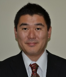
The Floating-Gate Memory from Concept to Flash Memory to the Fourth Industrial Revolution
Dr. Simon M. Sze, Honorary Chair Professor, NCTU
|
|
|
|
|
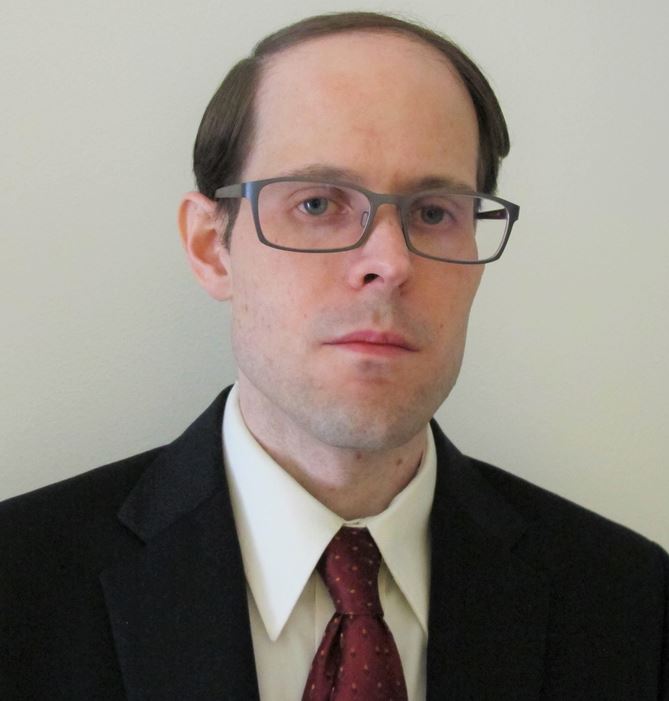
Moore's Law and Evolving Challenges in Technology Scaling
Dr. Yaoguo (Gary) Ding, Vice President, Intel
|
|
|
|
|
|
|
|
|
|
|
|
|
|
|
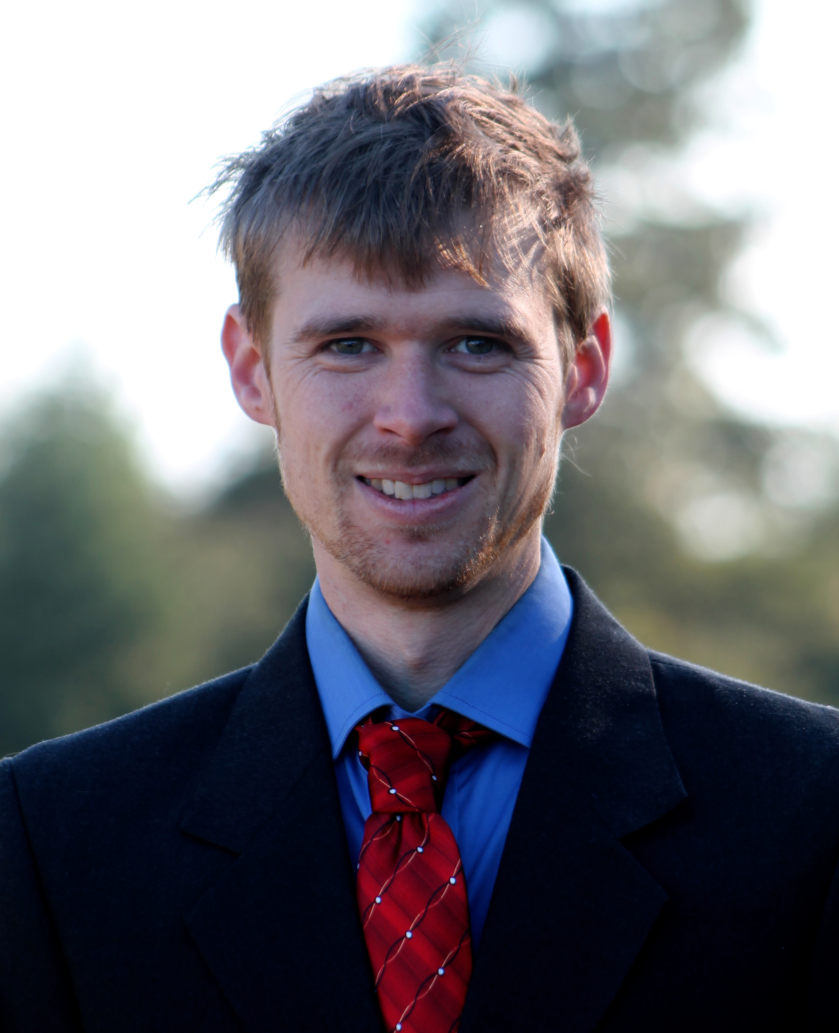
Semiconductor Innovation and Scaling: A Foundry Perspective
Dr. Min Cao, Vice President, Path-finding, TSMC
|
|
|
|
|
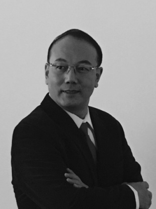
"In-memory Computing": Accelerating AI Applications
Dr. Evangelos Eleftheriou, Fellow, Neuromorphic Computing, IBM
|
Sponsored by:
|

|
|
|
|
|
|
|
|
|
|
|
|
|
|
|
|
|
|
|
|
|
|
Partial List of other Confirmed Distinguished CSTIC 2019 Invited Speakers
|
|
|
|
|
|
|
|
|
|
|
|
|
Accelerating Deep Neural Networks with Analog Memory Devices
Dr. Geoff Burr, IBM
|
|
|
|
|
Non-volatile Memory for Neuromorphic Computing
Prof. Sangbum Kim, Seoul Natioanl University
|
|
|
|
|
|
|
|
|
|
|
|
|
|
|
Defect Assessment in AlN Nucleation Layers Grown on Silicon and Silicon-on-Insulator Substrates
Eddy Simoen, IMEC
|
|
|
|
|
Fast Development of High-performance ICs in AI/IoT Era
Min-Hwa CHI, SiEn (Qindao) Integrated Circuits Cor.
|
|
|
|
|
|
|
Towards Efficient AI On-a-chip: Joint Hardware-algorithm Approaches
Prof. Yu Cao, Arizona State University
|
|
|
|
|
|
|
|
|
|
|
|
|
|
|
|
|
|
|
|
Scaling and Printing Electronics Using Nanomaterials
Prof. Aaron D. Franklin, Duke University
|
|
|
|
|
AC NEGF simulation: Efficient implementation and application to nanosheet MOSFETs
Prof. Sung-Min Hong, Gwangju Institute of Science and Technology
|
|
|
|
|
|
|
|
|
|
|
|
|
|
|
ReRam for alternative computing architectures
Prof. Khaled N. Salama, UCSD
|
|
|
|
|
Super steep switching CMOS device technology
Prof. Changhwan Shin, Sungkyunkwan University
|
|
|
|
|
|
|
|
|
|
|
|
|
|
|
Steep-Slope Hysteresis-Free Negative-Capacitance 2D Transistors
Prof. Peide Ye, Purdue University
|
|
|
|
|
Design & Technology Co-optimization for High Performance & Low Power Mobile SoC Productization
Dr. Jun Yuan, Qualcomm
|
|
|
|
|
|
|
|
|
|
|
|
|
|
|
New Understanding of Negative Capacitance Devices for Low-Power Logic Applications
Prof. Qianqian Huang, Peking University
|
|
|
|
|
Understanding the negative capacitance in nanoscale by two-dimensional phase field simulations
Cheol Seong Hwang, Seoul National University
|
|
|
|
|
|
|
|
|
|
|
|
|
|
|
Computing with Memristive Devices and Arrays
J. Joshua Yang, University of Massachusetts
|
|
|
|
|
Spin-Transfer-Torque Magnetic Random Access Memory: Co-Development of New Technologies and Architectures
Nuo Xu, Samsung Electronics
|
|
|
|
|
|
|
|
|
|
|
|
|
|
|
Novel gap filling BARC with high chemical resistance
Mr. Yuto Hashimoto, Nissan Chemical Corporation
|
|
|
|
|
High Power LPP-EUV Source with Long Collector Mirror Lifetime for Semiconductor High Volume Manufacturing
Dr. Hakaru Mizoguchi, Gigaphoton Inc.
|
|
|
|
|
|
|
|
|
|
|
|
|
|
|
Advances in IC Mask Synthesis and Tape Out Operations in the era of Machine Learning
Dr. Steffen Schulze, Mentor Graphics
|
|
|
|
|
Reduction and control of edge placement error at the 5nm node through a holistic approach
Dr. Robert Socha, ASML
|
|
|
|
|
|
|
|
|
|
|
|
|
|
|
Advanced Lithography Material Status toward 5nm Node and beyond
Dr. Koichi FUJIWARA, JSR Shanghai Co., Ltd.
|
|
|
|
|
Pattern fidelity control on EUV via hole towards 5-nm node
Hidetami Yaegashi, Tokyo Electron Limited
|
|
|
|
|
|
|
|
|
|
|
|
|
|
|
Multi-beam mask writer MBM-1000
Dr. Hiroshi Matsumoto, NuFlare Technology
|
|
|
|
|
EUV Lithography optics - current status and outlook
Dr. Dirk Juergens, Carl Zeiss SMT GmbH
|
|
|
|
|
|
|
|
|
|
|
|
|
|
|
EUV Mask near Field Synthesis
Taian Fan, IMECAS
|
|
|
|
|
Evolution of Lithographic Materials Enabling the Semiconductor Industry
Dr. Cheng-Bai Xu, DowDuPont
|
|
|
|
|
|
|
|
|
|
|
|
|
|
|
Tailoring Material and Process Variables to Control Planarization Properties at ≤ 7-nm nodes
Daniel M. Sullivan, Brewer Science
|
|
|
|
|
Study of CD-SEM based and other reference metrologies for line width roughness (LWR) control on EUV photoresist and less than 20nm width materials
Dr. Takeshi Kato, Hitachi High Technologies
|
|
|
|
|
|
|
|
|
|
|
|
|
|
|
Boosting Computational Lithography Performance with High Speed Metrology
and Machine Learning Technology
Dr. Gary Zhang, ASML-Brion
|
|
|
|
|
TBD
Will Conley, ASML-Cymer
|
|
|
|
|
|
|
|
|
|
|
|
|
|
|
How Curvilinear Mask Patterning will Enhance the Wafer Process Window: A Study Using Rigorous Wafer+Mask Dual Simulation
Ryan Pearman, D2S
|
|
|
|
|
Multi-Beam Mask Writer for Advanced Patterning
Naoya Hayashi, Dai Nippon Printing Co., Ltd.(DNP)
|
|
|
|
|
|
|
|
|
|
|
|
|
|
|
High Volume Semiconductor Manufacturing using Nanoimprint Lithography
Keita Sakai, Canon
|
|
|
|
|
Defectivity Reduction in EUV Lithography Materials using Advanced Filtration Technologies
Rao Varanasi, Pall Corporation
|
|
|
|
|
|
|
|
|
|
|
|
|
|
|
Thin Film Characterization for advanced patterning
Dr. Zhimin Zhu, Brewer Science
|
|
|
|
|
|
|
|
|
|
|
|
|
|
|
|
|
|
|
|
Development of A High Performance and Productivity ICP Etcher
Songlin Xu, Advanced Micro-Fabrication Equipment Inc.
|
|
|
|
|
Modeling and simulation approaches to atomistic control in etch and deposition processes: the role of surface modification and the catalytic nature of hydrogen
Dr. P. L. G. Ventzek, TEL
|
|
|
|
|
|
|
|
|
|
|
|
|
|
|
Towards the New Understanding of VHF Plasma Uniformity: Measurements of RF Magnetic Fields and Plasma Conduction Current in VHF Plasma Sources
Dr. Jianping Zhao, TEL
|
|
|
|
|
EUV SADP SAB Integration Scheme for Sub 30-nm Pitch Mx Patterning
Kiyotaka Imai, Tokyo Electron Limited
|
|
|
|
|
|
|
|
|
|
|
|
|
|
|
Challenges & Opportunities of Chamber Materials �For Chamber Productivity Enhancement
Jennifer Sun, Applied Materials, Inc
|
|
|
|
|
Advanced Etch Challenges and Perspective Solutions
Rich Wise, Lam Research, US
|
|
|
|
|
|
|
|
|
|
|
|
|
|
|
Atomic level surface treatment by down-stream plasma generated radicals
Hua Chung, Mattson Technology
|
|
|
|
|
Single Wafer Clean Challenges and Status
David Wang, ACM
|
|
|
|
|
|
|
|
|
|
|
|
|
|
|
A Patterning Solution for Perpendicular STT-MRAM by Utilizing Combined Etching
Dr. Dongchen Che, Leuven Instruments
|
|
|
|
|
Defect Control & Yield Improvement Using Advanced Filtration for Etch and Clean
David Huang, Pall (China) Co.,Ltd.
|
|
|
|
|
|
|
|
|
|
|
|
|
|
|
Advanced Device Challenges and the Solution from Etch
Joydeep Guha, AMAT
|
|
|
|
|
Advanced Si Etch System for 14nm and beyond
Tomoki Suemasa, Beijing NAURA Microelectronics Equipment Co. Ltd.
|
|
|
|
|
|
|
|
|
|
|
|
|
|
|
Precise Etching Profile Control by Atomic-Scale Process
Yoshihide Kihara, Tokyo Electron Miyagi Limited
|
|
|
|
|
|
|
|
|
|
|
|
|
|
|
|
|
|
|
|
Cobalt Electrofill for Future Generations of Contacts and Interconnects
Tighe Spurlin, Lam Research
|
|
|
|
|
Direct Copper Damascene Fill on Cobalt Liner Structures
Lee Brogan, Lam Research
|
|
|
|
|
|
|
|
|
|
|
|
|
|
|
Developments of Cu Barrier/liner Materials for 10nm CMOS Technology Node & Beyond
Dr. Xiaoping Shi, Naura
|
|
|
|
|
BEOL Low-k Dielectrics for 5nm and below
Dr. Kang Sub Yim, Applied Materials
|
|
|
|
|
|
|
|
|
|
|
|
|
|
|
Advanced Nanoscale Magnetic Tunnel Junctions for Low Power Computing
Prof. Weisheng Zhao, Beihang University
|
|
|
|
|
Advanced Ti-based silicides Ohmic contacts in sub-16/14 nm nodes
Dr. Jun Luo, IMECAS
|
|
|
|
|
|
|
|
|
|
|
|
|
|
|
Alternative metallization for advanced interconnects
Dr. Christoph Adelmann, IMEC
|
|
|
|
|
Integration Options for Enabling Fully Self Aligned Via
Gayle Murdoch, IMEC
|
|
|
|
|
|
|
|
|
|
|
|
|
|
|
3D hybrid scaling of CMOS for the next scaling era
Dr. Julien Ryckaert, IMEC
|
|
|
|
|
DFI™: Detect the Undetectable with Design for Inspection
Dr. Klaus Schuegraf, PDF Solutions
|
|
|
|
|
|
|
|
|
|
|
|
|
|
|
Enablement Strategies to minimize inputs of CMP process in Mass production
Dr. Ji Chul Yang, SK Hynix
|
|
|
|
|
The Characteristics of PVA Brushes in Post CMP Cleaning
Prof. Jin-Goo Park, Hanyang University
|
|
|
|
|
|
|
|
|
|
|
|
|
|
|
CMP mechanism of GISI multilevel interconnect
Chenwei Wang, Hebei University of Technology
|
|
|
|
|
Advances in CMP Formulations Technology
Dr. Hongjun Zhou, Versum materials
|
|
|
|
|
|
|
|
|
|
|
|
|
|
|
High rate ceria slurry and pad combo solution for bulk oxide CMP
Dr. Jinfeng Wang, Cabot Microelectronics
|
|
|
|
|
Ceria Slurry for Bulk Oxide and Selective CMP Applications
Dr. Xiansheng Yin, Anji Microelectronics Technology (Shanghai) Co. Ltd.
|
|
|
|
|
|
|
|
|
|
|
|
|
|
|
A Study on the Mechanical Role of Pad Asperities in Chemical-Mechanical Polishing
Prof. Sanha Kim, Korea Advanced Institute of Science and Technology
|
|
|
|
|
Beyond Planarization, into the Realm of Multifunctional Polishing
Dr. Hong Jin Kim, Globalfoundries
|
|
|
|
|
|
|
|
|
|
|
|
|
|
|
Study and Improvement on Tungsten Recess in CMP Process
Dr. Lei Zhang, Shanghai Huali Microelectronics Corporation
|
|
|
|
|
Opportunities and Challenges of CMP technology
for advanced memory manufacturing
Dr. Yukiteru Matsui, Toshiba Memory Corp.
|
|
|
|
|
|
|
|
|
|
|
|
|
|
|
Study on CMP Slurry with Graphene Oxide for Monocrystal SiC Wafer Polishing
Chao-Chang Chen, National Taiwan University of Science and Technology
|
|
|
|
|
The surface investigation of nano silica for CMP
Weili Liu, SIMIT
|
|
|
|
|
|
|
|
|
|
|
|
|
|
|
Post CMP Cleaning: Challenges and Defect Improvement Approaches
Katrina Mikhaylich, AMAT
|
|
|
|
|
Numberical simulation of marangoni drying in post-cmp clenaing
Dr. Dewen Zhao, Tsinghua University
|
|
|
|
|
|
|
|
|
|
|
|
|
|
|
Reliability challenges for advanced interconnect systems
Dr. Kristof Croes, IMEC
|
|
|
|
|
The Hype, Myths, and Realities of Testing 2.5D/3D Integrated Circuits
Prof. Krishnendu Chakrabarty, Duke University
|
|
|
|
|
|
|
|
|
|
|
|
|
|
|
Reliability Verification: Why it is complex, important and beneficial?
Sridhar Srinivasan, Mentor Graphics
|
|
|
|
|
TBD
Gary Ditmer, Lam Research
|
|
|
|
|
|
|
|
|
|
|
|
|
|
|
Comprehensive 3D Process Control
Jason Shields, Lam Research
|
|
|
|
|
|
|
|
|
|
|
|
|
|
|
|
|
|
|
|
High-resolution Time-domain Reflectometry Analysis in Back-End-of-Line (BEOL) by Recursive Circuit Modeling
Dr. Yang Shang, Advantest Singapore Pte Ltd
|
|
|
|
|
SCR Devices with Embedded RC triggering structure for ESD Protection
Dr. Zhiwei Liu, University of Electronic Science and Technology
|
|
|
|
|
|
|
|
|
|
|
|
|
|
|
High Performance Computing GPU and AI Packaging
Scott M and MC Hsieh, JCET
|
|
|
|
|
Advanced Process Development for System-Like HD SiP
Mike Zhao, ASE
|
|
|
|
|
|
|
|
|
|
|
|
|
|
|
Technology Development and Challenges of Power Packaging
Wayne Lin, TFME
|
|
|
|
|
Development of 3D Embedded Silicon Integration Technology
Daquan Yu, HuaTian Technology
|
|
|
|
|
|
|
|
|
|
|
|
|
|
|
Advance MIS Technology Development
Eric Zhu, JCET
|
|
|
|
|
Wafer Level Packaging - A mid-end approach
Liu Hong Jun, China Wafer Level CSP Co., Ltd
|
|
|
|
|
|
|
|
|
|
|
|
|
|
|
Analysis Methods for High Purity Sputtering Target Materils
Xueze Wang, KFMI
|
|
|
|
|
High Thermal Conductive DA Development
Tim Chen, Yantai Darbond Technology
|
|
|
|
|
|
|
|
|
|
|
|
|
|
|
Substrate Based PLP Technology
Lingwen Kong, Shennan Circuits Company Limited (SCC)
|
|
|
|
|
Advanced Packaging and the Materials Challenges
Fay Hua
|
|
|
|
|
|
|
|
|
|
|
|
|
|
|
Heterogeneous Integration Roadmap Driving Force and Enabling Technology for Systems of the Future
Bill Chen and Bill Bottoms, ASE Fellow
|
|
|
|
|
Low-Power AI Chips for Edge Computing
Dr. Kirby Li, Qualcomm
|
|
|
|
|
|
|
|
|
|
|
|
|
|
|
How to Successfully Overcome Inflection Points by Using the Technology Roadmap Methodology
Dr. Paolo A. Gargini, International Roadmap for Devices and Systems (IRDS)
|
|
|
|
|
Challenges in Circuit
Designs and Devices-Circuits Interaction for Computing-in-Memory
Dr. Meng-Fan (Marvin) Chang, National Tsing Hua University
|
|
|
|
|
|
|
|
|
|
|
|
|
|
|
Process Overview of Area-Selective Deposition; Surface-Determined Patterning Technology toward Advanced Nanofabrication
Prof. WooHee Kim, Jeonbuk National University
|
|
|
|
|
Hybrid Solid State Chemoresistive and Fluctuation-Enhanced Gas Sensors: Exhaled Breath and Indoor Air Analysis
Tesfalem Welearegay, Uppsala University
|
|
|
|
|
|
|
|
|
|
|
|
|
|
|
A novel gate junction design for low noise Si Nanowire ISFET Sensors
Prof. Zhen Zhang, Uppsala University
|
|
|
|
|
Analog Resistive Switching Memory for Neural-Network Processing Unit
Prof. Bin Gao, Hsinghua University
|
|
|
|
|
|
|
|
|
|
|
|
|
|
|
Development of Thin Film Technologies for IoT and Smart Society
Dr. KouKou Suu, ULVAC
|
|
|
|
|
AI: From Deep Learning to In-Memory Computing
Hsiang-Lan Lung, Macronix
|
|
|
|
|
|
|
|
|
|
|
|
|
|
|
The implementation of semiconductor based biosensors into Point of Need systems for the automatized analysis of complex samples
Sascha Geidel, Fraunhofer ENAS
|
|
|
|
|
Current Progress on 2D Materials and their FETs for Future LSIs
Prof. Hitoshi Wakabayashi, Tokyo Institute of Technology
|
|
|
|
|
|
|
|
|
|
|
|
|
|
|
The Life of SPICE as A Transient Circuit Simulator
Prof. Chung-Kuan Cheng, UC San Diego
|
|
|
|
|
Edge Computing
for Intelligent Healthcare
Prof. X. Sharon Hu, University of Notre Dame
|
|
|
|
|
|
|
|
|
|
|
|
|
|
|
Design, Implementation and Integration for Smart Headlights
Prof. Xin Li, Duke University
|
|
|
|
|
DTCO is the New Moore’s Law for Advanced Logic and Memory
Dr. Victor Moroz, Synopsys Inc.
|
|
|
|
|
|
|
|
|
|
|
|
|
|
Overview of A FPGA-based Overlay Processor
Prof. Lei He, UC Los Angeles
|
|
|
|
|
Not Your Father's Timing Anymore – Novel Approaches to Timing of Digital Circuits
Prof. Ulf Schlichtmann, Technical University of Munich
|
|
|
|
|
|
|
|
|
|
|
|
|
|
|
Computing-in-Memory for Binary Neural Networks
Prof. Shimeng Yu, Georgia Institute of Technology
|
|
|
|
|
Nanometer Analog Circuit Synthesis by Multi-objective Bayesian Optimization
Prof. Xuan Zeng, Fudan University
|
|
|
|
|
|
|
|
|
|
|
|
|
|
|
Dadu - Processor Design for Robot
Prof. Yinhe Han, Institute of Computing Technology, Chinese Academy of Science
|
|
|
|
|
Design Automation of Digital Microfluidic Biochips
Prof. Krishnendu Chakrabarty, Duke University
|
|
|
|
|
|
|
|
|
|
|
|
|
|
|
Accelerate Analog Circuit Simulation
Senhua Dong, Huada Emprean Inc.
|
|
|
|
|
A 1μw-to-100μw Output Range Boost DC-DC with Pseudo Open Loop Structure and Power Efficient Ring Oscillator
for Wireless Energy Harvesting
Prof. Le Ye, Peking University
|
|
|
|
|
|
|
|
|
|
|
|
|
|
|
AI Vision Processor for the Automotive - from Horizon
Dr. Davids Wu, Horizon Shanghai IC Design Center
|
|
|
|
|
|
|
|
|
|
|
|
|
|
|
|
|
|