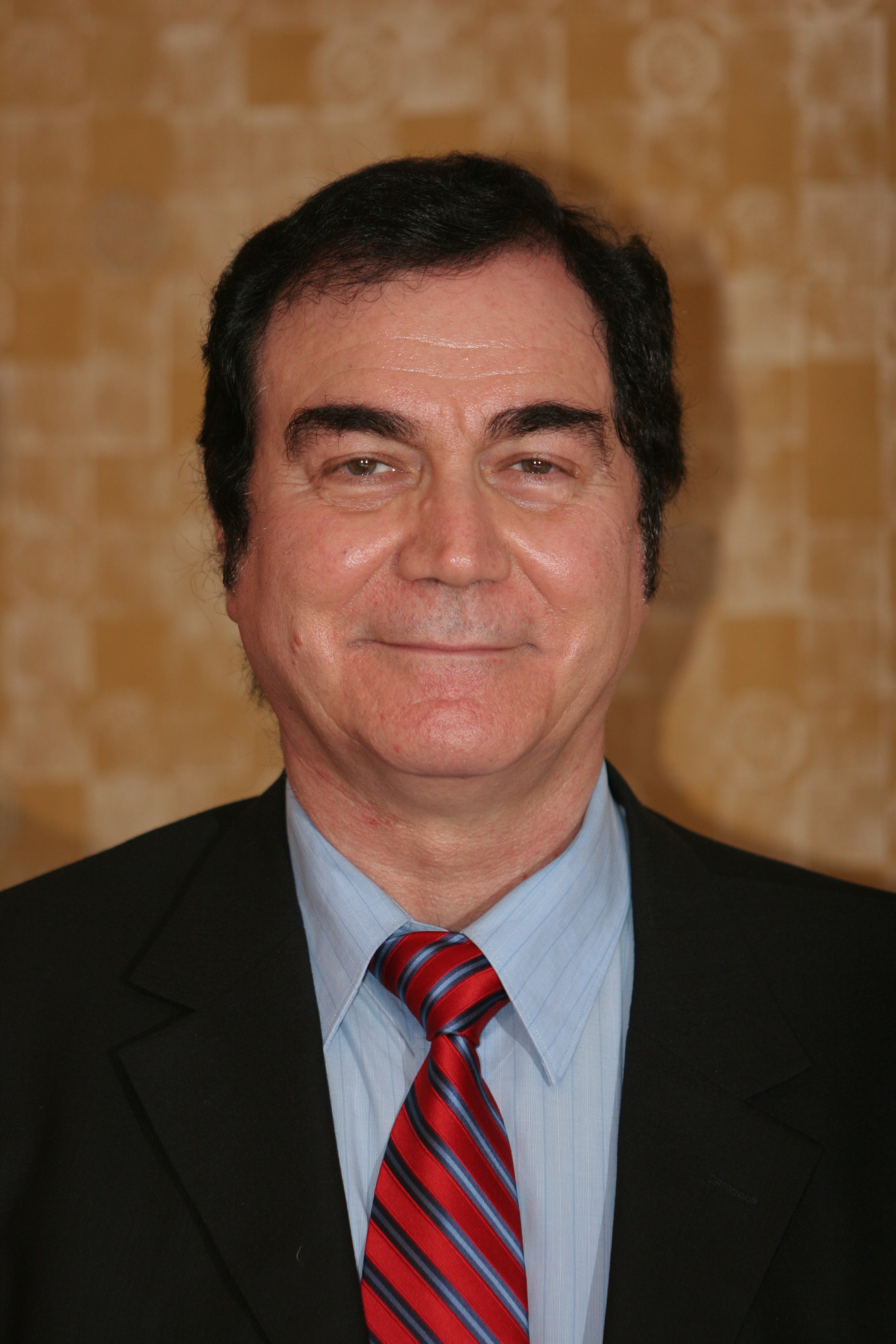
|
Dr. Gargini was born in Florence, Italy and received a doctorate in Electrical Engineering in 1970 and a doctorate in Physics in 1975 from the Università di Bologna, Italy, both with full honor and marks.
He has done research at Stanford University and at Fairchild Camera and Instrument (Research and Development) in Palo Alto in the early 70s.
Since joining Intel in 1978 he was responsible for Microprocessor technology including 80286 and the 80386 processors. In 1985 he headed the first submicron process development team at Intel. He was also responsible for all equipment selections from 1994 to 2007.
In 1996, Dr. Gargini was elevated to Director of Technology Strategy, Intel Fellow.
He was responsible for worldwide consortia research for the Technology and Manufacturing Group (TMG) from 1993 to 2012; he was member of Sematech, SRC and SIA Boards.
Thorough the years Dr. Gargini successfully transferred the foundations of fundamental technologies into Intel such as: Copper interconnects, 248nm and 193nm lithography, Strained Silicon, High-K/Metal-Gate, FinFET and many new materials.
From 1998 to 2015, Dr. Gargini has been the Chairman of the International Technology Roadmap for Semiconductors (ITRS) sponsored by the WSC. Since 2016 he is the Chairman of the International Roadmap for Devices and Systems (IRDS) sponsored by IEEE.
Dr. Gargini became the first Chairman of the Governing Council of the Nanoelectronics Research Initiative (NRI) funded in June 2005 by SIA.
He is co-chairman of the EUVL Symposium.
Dr. Gargini was inducted in the VLSI Research Hall of Fame in 2009.
Dr. Gargini was elevated to IEEE Fellow in 2009 and to International Fellow of the Japan Society of Applied Physics in 2014.
Dr. Gargini is chairman of ETAB of E3S (UCB); he is also a member of NEREID Advisory Board (ETAB) for the European Roadmap.
He is a member of the leadership committee of the IEEE initiative on Future Networks aimed at 5G and Beyond Roadmap.
|