| Date: | Tuesday, March 19, 2019 |
| Venue: | Shanghai International Convention Center |
| Room: | 5F |
| 在线登记 | |
|
|
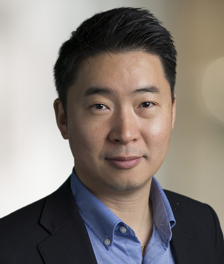
14:30-15:30 Materials Engineering Driven Solution for 3D NAND Technology and Its Scaling Dr. Sean KangDirector, Applied Materials
Biography |
|
|
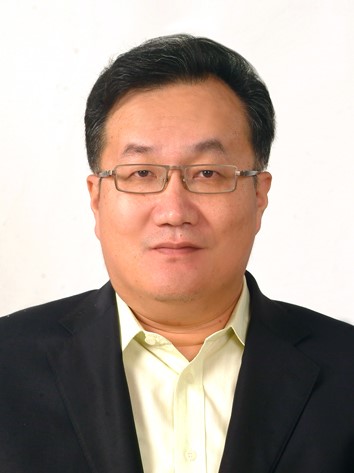
15:30-17:00 Exploring the Best Memory Solution : DRAM & PCM Dr. Hongsik JeongProfessor in Tsinghua University
Biography He received the Korean presidential award due to the achievement of worldwide leadership of new memory devices in 2005. And then he was promoted as a Vice President in Samsung Semiconductor R&D Center and Memory Business Division. He had led various TF teams from MRAM on verification level to PRAM and FRAM on the product level. Finally, PRAM had been succeeded in development for production, world first 82nm, 58nm and 39nm technology node 1Gb PRAM devices for mobile phone application have been developed and launched successfully under his leadership until 2013. In 2014, he moved to Yonsei University in Korea as a research professor studying the new concept of computing based on new memory devices. Since 2016, he has studied neuromorphic devices for AI applications as a professor of EE department and CBICR (Center for Brain-Inspired Computing Research) in Beijing, China. He has also contributed international new memory society as a key person for enhancing collaboration between worldwide new memory researchers. He has published 1 chapter of a book, over 120 technical papers, 40 patents and given over 30 presentations in international conferences as a keynote and invited speaker. |