|

|
中国国际半导体技术大会(CSTIC) 2018
China Semiconductor Technology International Conference (CSTIC) 2018
Plan now to participate at CSTIC 2018, one of the largest and the most comprehensive annual semiconductor technology conferences in China and Asia since 2000. Organized by SEMI, IMEC and IEEE-EDS, co-organized by IMECAS. CSTIC 2018 will be held March 11-12, 2018 in Shanghai, China, in conjunction with SEMICON China 2018. The conference will have nine symposiums cover all aspects of semiconductor technology with focus on manufacturing and advanced technology, including detail manufacturing processes, devices design, integration, materials, and equipment, as well as emerging semiconductor technologies, circuit design, and silicon material applications. Hot topics, such as memory technology, 3D integration, MEMS Technology will also be addressed in the conference.
**Full length manuscripts of accepted papers will be considered for publication in IEEE Xplore.
Date and Venue
|
March 11-12, 2018 Shanghai International Convention Center 上海国际会议中心 中国上海浦东滨江大道2727号 No.2727 Riverside Avenue Pudong, Shanghai 200120, China |

|
||||
Distinguished Conference Keynote Speakers
Conference Chairman
 |
Dr. Ru Huang Peking University, China
|
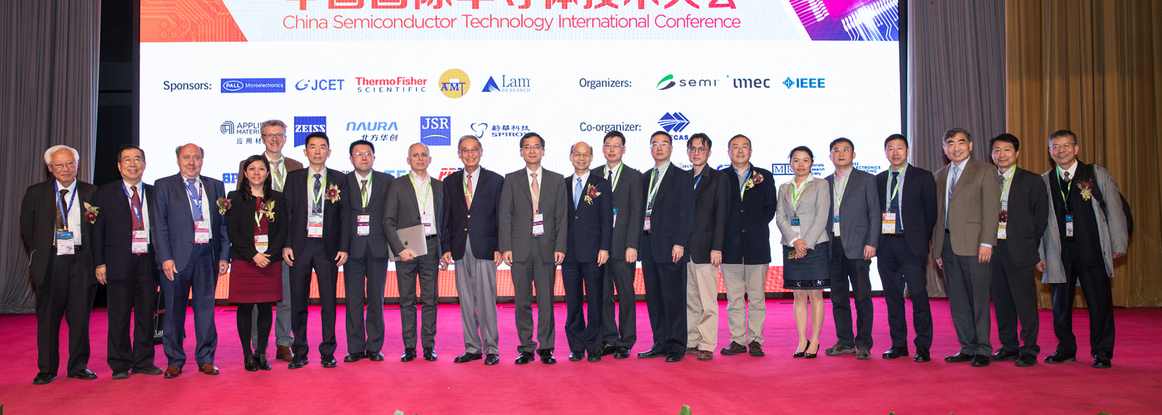
CSTIC 2018 Post Conference Report
| Platinum Sponsor: |

|
| Gold Sponsor: |

|

|
| Silver Sponsor: |

|

|

|

|

|
|

|

|
|

|
|
||
|
|

|
|
|
| Bronze Sponsor: |

|

|

|
| Organizer: |

|

|

|
| Co-organizer: |
|
| Co-sponsor: |
|

|

|

|
| Proceedings Publication: |
|
Partial list of other confirmed distinguished CSTIC 2018 invited speakers
| III-V GaAs and InP HBT device for 4G & 5G wireless applications |
| Colombo R. Bolognesi, Prof., Eidgenössische Technische Hochschule Zürich |
| CMOS Scaling – Past, Present, and Future |
| Kangguo Cheng, Senior Technical Staff Member, IBM |
| Negative capacitance: principle, practice, and limitation |
| Cheol Seong Hwang, Prof.,Seoul National University |
| Emerging Three-dimensional Memory Technologies |
| Yoon Kim, Prof., Pusan National University |
| Device and Process Technologies for Extending Moore's Law |
| Sangwan Kim, Prof., Ajou University |
| Innovative graphene-based remote epitaxy & layer transfer-EPI growth & Device Applications |
| Jeehwan Kim, Prof., Massachusetts Institute of Technology |
| Investigation of Hysteresis Phenomena in 3-D NAND Flash Memory Cells Using Pulse Measurement |
| Jong-Ho Lee, Prof., Seoul National University |
| Nonvolatile Memory Outlook: Technology driven or Application driven |
| Jing Li, Dr., University of Wisconsin-Madison |
| ACTIVE-PERFORMANCE BENCHMARK FOR ADVANCED 3D-CMOS DEVICES |
| Hitoshi Wakabayashi, Prof., Tokyo Institute of Technology |
| FEOL Reliability in Advanced FinFET Technologies |
| Miaomiao Wang, Dr., IBM |
| Emulation of the human brain by nanodevices at different scales |
| Yuchao Yang, Assistant Professor, Peking University |
| Unconventional computing with memristive neural networks |
| Joshua Yang, Prof., University of Massachusetts |
| Predictive As-grown-Generation model for NBTI of advanced CMOS devices and circuits |
| Zhijiang Ji, Dr., Liverpool John Moores University |
| Opposite trends between digital and analog performance for different TFETs technologies |
| Paula Ghedini Der Agopian, Assistant Prof., Sao Paulo State University (UNESP) |
| Confined Phase Change Memory for M-type Storage Class Memory |
| Wanki Kim, Dr., IBM |
| Applications Of Organic Semiconductors And Recrystallized Silicon Devices |
| Ioannis (John) Kymissis, Prof., Columbia University |
| MTJ-Based Nonvolatile Logic LSI for Ultra Low-Power and Highly Dependable Computing |
| Masanori Natsui, Prof., Tohoku University |
| Do we have to worry about extended defects in high-mobility materials |
| Eddy Simoen, Prof., IMEC/University of Ghent |
| Design-process co-optimization for system improvement |
| Da Zhang, Dr., AMD-China JV |
| Nanosheet Transistor for 5nm Technology and Beyond Aiming High Performance and Low Power Applications |
| Huiming Bu, Dr., IBM |
| Phase-change-memory devices for non-von Neumann computing |
| Evangelos Eleftheriou, Fellow, IBM |
| Desirable material selection on Self-aligned Multi-patterning |
| Hidetami Yaegashi, Manager, TEL |
| Advanced CD-SEM metrology for Process control of 14 nm-node HVM and beyond. |
| Takeshi Kato, Senior Engineer, Hitachi High Technologies |
| Accessing light source driven contrast variation impact on hotspots using Lithography Manufacturability Checker (LMC) |
| Will Conley, Staff Applications Mgr, ASML-Cymer |
| Machine Learning for Computational Lithography |
| Yu Cao, CEO, ASML-Brion |
| Sketch and Peel Lithography for Multiscale Patterning |
| Huigao Duan, Prof. Hunan University |
| Advanced Lithography Material Status toward 7nm Node and beyond |
| Kouichi Fujiwara, General Manager, JSR |
| Close – loop – design and manufacturing optimization for advanced nodes |
| Steffen Schulze , Sr. Director of Marketing, Mentor Graphics |
| Resist Model Setup for Negative Tone Development at 14nm Node |
| Lijun Zhao, Process Engineer, IME |
| High Power LPP-EUV Source with Long Collector Mirror Lifetime for High Volume Semiconductor Manufacturing |
| Hakaru Mizoguchio, Executive Vice President, CTO, Gigaphoton Inc. |
| Robust overlay metrology by Mueller matrix ellipsometry with a differential calculus |
| Xiuguo Chen, Assistant Prof., HUST |
| Technical issues of scanner used in packaging |
| Huang Dongliang,SMEE |
| Advanced Photoresist and Material development in China |
| Yusong Sun, VP, Hantop |
| Multi-beam mask writer MBM-1000 |
| Hiroshi Matsumoto, Chief Engineer, NuFlare |
| Display photomask requirements have reached a new level and matches low end semicon |
| Robert Eklund, Senior Specialist, Mycronic |
| Full-chip GPU-Accelerated Curvilinear Dose and Shape Correction for EUV Photomasks |
| Ryan Pearman, Chief Scientist, D2S |
| Lithography simulations for flat panel display manufacturing |
| Thomas Muelder, R&D engineer, Synopsys |
| Machine Learning for Lithography and Physical Design |
| David Pan, Prof., University of Texas at Austin |
| Advanced Topcoat and Embedded Barrier Layer (EBL) for 193nm Immersion Lithography |
| Cong Liu (Colin), Research Scientist/R&D Manager, Dow Chemical |
| High fedelity lithography against stochastic effects |
| Zhimin Zhu, Senior Scientist, Brewers science |
| Inter-mask effects in EUV lithography |
| Christopher Progler, Chief Technology Officer, Photronics Inc |
| Patterning challenges and opportunities for Advanced Memory Technology |
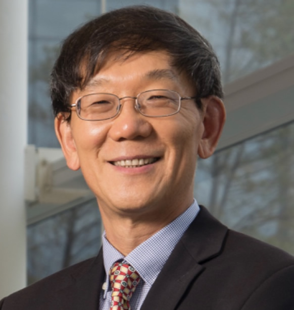
| Gill Lee, PPG CTO, AMAT |
| Memory Patterning Roadmaps |
| Siva Kanakasabapathy, APTD BEOL Technologist, Lam Research |
| Patterning for beyond 14nm nodes |
| Lei Zhong, GF Account Technology Director, AMAT |
| Patterning Roadmap |
| Rich Wise, Patterning Managing Director, Lam Research |
| Advanced Etch Technology for Patterning 14nm and beyond |
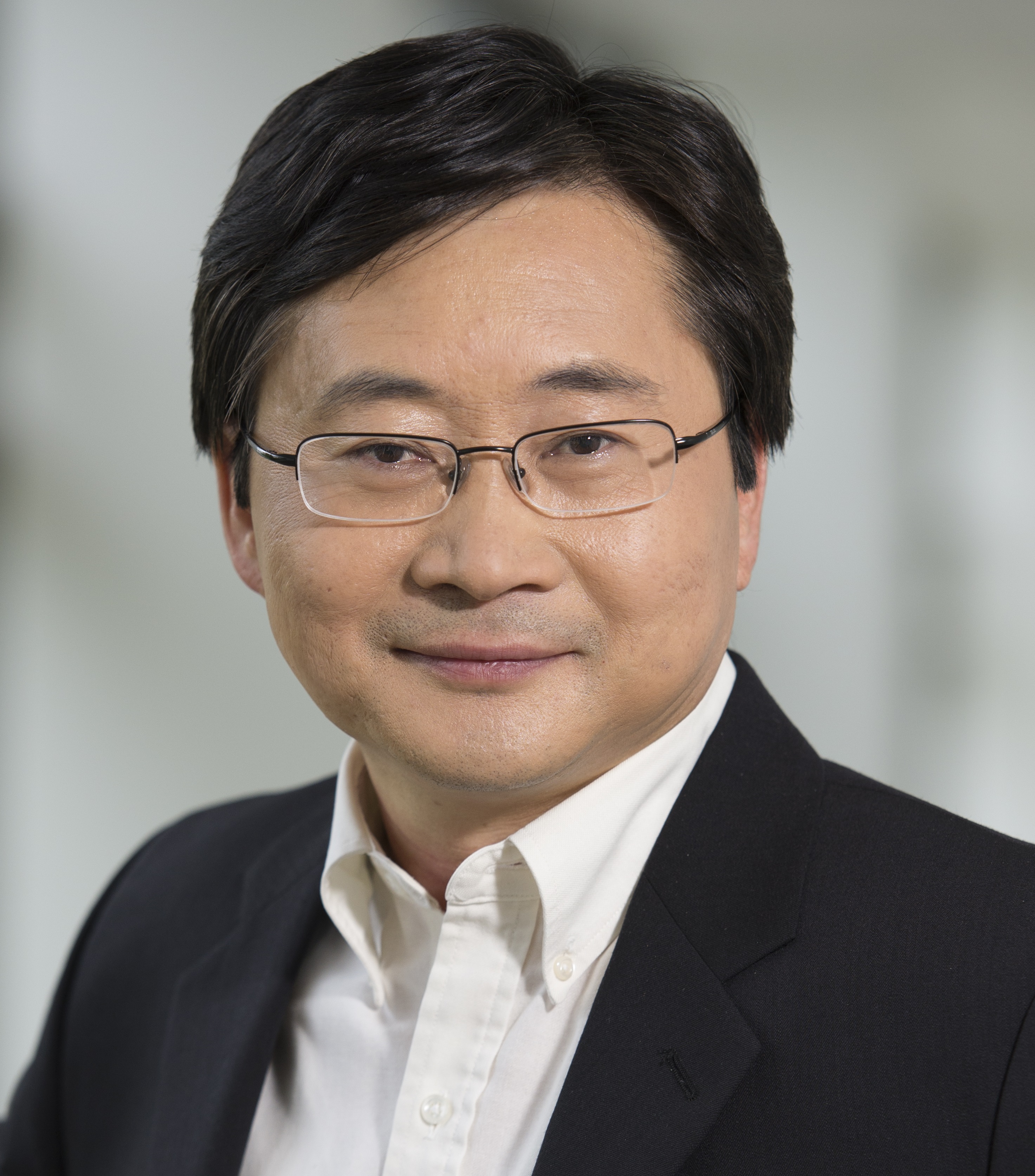
| Ying Huang, Dr., AMAT |
| SAQP and SAOP for 5nm nodes and beyond |
| Dr. Efrain Altamirano Sanchez, Manager, IMEC |
| Patterning Technology Options for Future Scaling |
| Kenichi Oyama, Project Leader and Director, TEL |
| Benefits of atomic-level processing by Quasi-ALE and ALD technique |
| Masanobu Honda, Director of Advanced Process development Laboratory, TEL |
| Atomic Layer Etch Modeling for Advanced Patterning |
| Peter Ventzek, TEL |
| Major Challenges and Proposed Solutions for Critical Etch Applications with Inductive Coupled Plasma |
| Shenjian Liu, Deputy GM Conductor Etch, AMEC |
| Resist Strip Technology for Advanced Technology Nodes |
| Ma Shawming, Senior Director, Mattson |
| Advanced Selective Dry Etching of Silicon Based Materials and Cobalt |
| Jun Lin, Dr., TEL |
| A High Performance Patterning Solution by Utilizing Combined Etching for Perpendicular STT-MRAM |
| Kaidong Xu, CEO, Leuevn Instrument |
| Materials/Process Innovations required for High Performance BEOL interconnects |
| Griselda Bonilla,Senior Technical Staff Member, Senior Manager, Advanced BEOL Interconnect Technology, IBM |
| Electrochemical ALD - A New Paradigm for Enabling Aggressive Scaling in BEOL Interconnect Metallization |
| Yezdi Dordi, Director, Lam Research |
| Co alloy for Middle of Line for Fin FET of sub-7 nm |
| Junichi Koike, Prof., Tohoku University |
| Extension of 14nm FinFET Technology with High Performance, Ultra Low Power and High Density for Different Applications |
| Owen Hu, Deputy director, Global fundry |
| Fully Printable and Autonomously Powered Electronic Nodes for the Internet of Everything |
| Paul Berger, Prof., Ohio State University |
| Metal Interconnect Considerations for Logic 5 nm Node and Beyond |
| Steve Lai, Director, Lam Research |
| All-ALD high-k/metal gate as an enabler for FinFETs and nanowire FETs |
| Zhao Chao, Research Prof., IME |
| Flexible Silicon/Germanium Nanomembranes for Integrative 3D Devices |
| Yongfeng Mei, Prof., Fu Dan University |
| Plasma enhanced ALD technology & worldwide applications |
| Toshihisa Nozawa, R&D VP, ASM |
| Thin Film Process Technologies for Continued Scaling |
| Robert Clark, Manager, TEL |
| PVD Systems for Advanced Packaging Applications |
| Peijun Ding, Director, Naura |
| Overview of ALD Applications for Advanced CMOS Technology |
| Xiaoping Shi, Technical Director, Naura |
| Low Temperature Microwave Annealing for CMOS Scaling |
| Bharat Krishnan / Rinus T.P. Lee, Manager for diffusion module, Global fundry |
| In-situ plasma monitoring of PECVD nano-crystalline a-Si:H(i)/ a-Si:H (n) surface passivation for Heterojunction Solar cells Application |
| Yiin-Kuen Fuh, Prof., National Central University |
| Patterning Challenges in 193i-based Tip to Tip in N5 Interconnects |
| Basoene Briggs, Senior R&D Engineer, IMEC |
| CMP Challenges for Advanced Logic and Memory Device Manufacturing |
| Sidney Huey, Global Product Manager, AMAT CMP |
| CMP technology for advanced package |
| Haedo Jeong, Prof., Pushan University |
| New CMP tool Development and Its Applications |
| Dewen Zhao, Faculty, Tsinghua University |
| Colloidal Silica: Chemistry, Properties and Adaptations for Electronic Polishing Applications |
| Francois Batllo, RD director, Nalco |
| CMP Challenges to Keep Up with Moore’s Law |
| Gary Ding, TD Engineering Manager, Intel Corporation |
| CMP Challenges for Interconnect Scaling |
| Donald F Canaperi, Manager, IBM |
| Defect control for high k metal gate CMP |
| Changhong Gong, TD3 department manager, Huali |
| Slurry Filtration for CMP Defect Improvement |
| David Huang, Director, Pall |
| Co-optimization of CMP Pad and Slurry for Overall Process Performance Enhancement |
| Robert Auger, Asia Technology Site Leader and Slurry R&D Director, Dow |
| From Confined Area to Wafer Level Nanotopography Metrology Solution for Process Developments |
| Tae-Gon Kim, senior researcher, IMEC |
| Continuous Process Control for Metal CMP |
| Jianshe Tang, AMAT CMP |
| Middle of Line Contact for Advanced Node Semiconductor: from Tungsten to Cobalt |
| Stan Tsai, Technology Research, GLOBALFOUNDRIES |
| CMP New Challenges in 3D NAND Era |
| Ke K. Wang, Engineering Manager, Intel Dalian |
| Slurry development in sapphire,SiC, Si, and LiTaO3 |
| Weili Liu, Shanghai Institute of Microsystem and Information Techology |
| ALD W metal gate CMP |
| Tao Yang, Associate Prof., IME |
| Challenges and Solutions in Today’s Safety Critical SOCs |
| Yervant Zorian, Chief Architect and Fellow at Synopsys, President of Armenia, Synopsys |
| Reliability Engineering: Help Enable Technology Scaling |
| Sangwoo Pae, VP of Quality & Reliability at Samsung Foundry, Samsung's |
| Applications of Advanced Techniques of Transmission Electron Microscope in Characterizations of Semiconductor Devices |
| Jinghong Li, Principle Member of Technical Staff, GLOBALFOUNDRIES |
| Assessing the accuracy of statistical properties extracted from a limited number of device under test for time dependent variations |
| J.F. Zhang, Prof., Liverpool John Moores University |
| Machine Learning Enabled in situ Etch Endpoint Control |
| Ye Feng, Director, Lam Research |
| Improvement of Package Warpage through Substrate and EMC Optimization |
| Ken Lee, CTO, Simmtech, Co., Ltd. |
| FAN-OUT WAFER-LEVEL PACKAGING FOR 3D IC HETEROGENEOUS INTEGRATION |
| John H Lau, Senor Technical Advisor, ASM Pacific Technology |
| STRUCTURING REDISTRIBUTION LAYERS DOWN TO 2 MICRON LINE SPACING WITH LASER DIRECT ABLATION |
| Dirk Müller, Director, Coherent |
| Emerging fine line panel level fan out technology |
| David Fang, CTO and RD VP, Powertech Technology Inc. (PTI). |
| Packaging and Integration Strategy for mmWave Products |
| SW Yoon, JCET/STATSChipPAC |
| New Wave SiP for mmWave |
| Dr. KK Kuo, Senior Director, Engineering Center, ASE |
| Driving into the Innovation World – Amkor’s Automotive Package Solution |
| John Lee, Amkor |
| New Developments in Advanced MIS Packaging |
| YB Lin, JCET |
| TBD |
| Fan Chun Ho, ASM Pacific |
| Polyimide applications and development in advanced packaging |
| Shian Shen, Taiflex Scientific (/NCTU) |
| Toward chemoresistive ssensor array based on two-dimensional materials |
| Ho Won Jang, Prof., Seoul National University |
| CMOS Integrated Lab-on-chip System for Personalized DNA Sequencing |
| Hao Yu, Prof., Southern University of Science and Technology |
| Implantable Optoelectronic Devices for Deep-Brain Neural Modulation and Sensing |
| Xing Sheng, Prof., Tsinghua University |
| The development of micro-machined based electrochemical seismic sensors |
| Junbo Wang, Prof., Institute of Electronics, Chinese Academy of Sciences |
| The Two-fold Role of Connected Devices — Enabling remote healthcare service delivery & healthcare service innovations |
| Zhen Fang, Prof., Institute of Electronics, Chinese Academy of Sciences |
| MEMS Sensors for Oceanic Applications |
| Chenyang Xue, Prof., North University of China |
| RF MEMS resonant devices for wireless communication |
| Jinling Yang, Prof., Institute of Semiconductors, CAS |
| Application driven Technologies Beyond Scaling |
| Meikei Ieong, CTO, ASTRI, Hong Kong |
| Research Achievements of Key Technologies in 3D Integration and Heterogeneous Integration |
| Kuan-Neng Chen, Prof., National Chiao Tung University |
| Synthesizing Large-area Two-Dimensional Molybdenum Ditelluride by Physical Vapor Deposition and Solid-phase Crystallization |
| Tuo-Hung Hou, Prof., National Chiao Tung University |
| SiGe epitaxial memory for neuromorphic computing |
| Jeehwan Kim, Prof., MIT, USA |
| All-silicon Micro-Fabricated High-Temperature High-Pressure Sensor |
| Man WONG, Prof., The Hong Kong University of Science and Technology |
| Low-frequency noise originating from the dynamic hydrogen ion reactivity at the solid/liquid interface of ion sensors |
| Zhen Zhang, Associate Prof., Uppsala University |
| ThirdEye : Visual Assist for Grocery Shopping |
| Vijay Narayanan, Prof., Pennsylvania State University |
| Novel Approaches to Circuit Timing |
| Ulf Schlicthmann, Prof., Technical University of Munich |
| MTTF-aware Design Methodology for Adaptive Voltage Scaling |
| Masanori Hashimoto, Prof., Osaka University |
| Electrical and thermal characterization of SiC power MOSFETs |
| Takashi Sato, Prof., Kyoto University |
| An accelerator-aware microarchitecture simulator for design space exploration |
| Cheng Zhuo, Prof., Zhejiang University |
| Optimizing Stochastic Number Generators for Stochastic Computing |
| Weikang Qian, Assistant Prof., Shanghai Jiaotong University/University of Michigan |
| Statistical Validation for Autonomous Driving Systems |
| Xin Li, Prof., Duke University & Duke Kunshan University |
| Which Neural Networks are the “Best”? - -- A case study of technology, circuit and architecture impacts on the MNIST Dataset |
| Sharon Hu, University of Notre Dame |
| How to Obtain and Run Light and Efficient Deep Learning Networks |
| Yiran Chen, Duke University |
| Award winner presentation |
| Yier Jin, University of Florida |
| Making Aging Useful: A Novel Wake-up Scheduling Approach |
| Yuguang Chen, Yuan Ze University |
CSTIC 2018 Agenda
Keynote & Invited Speakers
Keynote & Invited Speakers (2018)
Contact Us
Kelly Zhang, SEMI China
Tel: 86.21.6027.8556
Fax: 86.21.6027.8511
Email: [email protected]